Micromachining of semiconductors

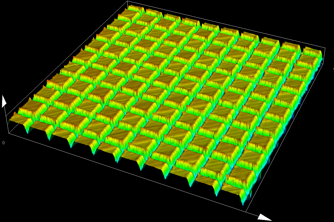
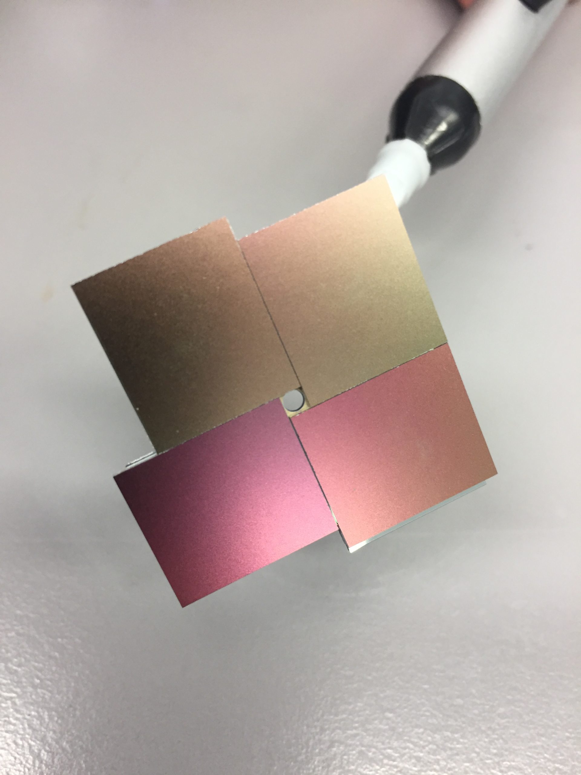
The new technology of laser cutting, drilling and micromachining of semiconductors used in sensors: – Process without affecting sensor characteristics such as leakage current – The ability to process the sensor on the entire assembly (ROC+Sensor) without damaging neighbouring pixels – The thickness of the machined material  from 100, 300 to 500 µm – The possibility of arbitrary sensor shape …

3D laser stripping

developed for monolithic cutting tools, where multi-axis kinematics is applied detailed info will be added soon

Microparts

Focused on crucial details Small dimensions in order of tenths of millimeters up to units of micrometers Fine surface roughness < 0,2µm our laser systems enable to reach fine quality surface roughness (<0,2 µm) in combination of very tight tolerance field (+/- 2 µm). Smaller tolerances can be considered  after consultation.

IMG_6781_1_cut
IMG_9615_cr
IMG_9658_cr_C

Chip breakers for cutting tools

combines radial or tangential way of laser micromachining with highly accurate 5-axis stages in combination of 2-axis optical galvo-scanner. For this type of micromachining a recognition interface via camera is needed as an in-machine measurement, which helps very pricesily to identify general freeform planes of products (e.g. monolitnic cutting tools, micro-parts,…).

Polygon_C
square_C
Dots_C
Shark_c

Surface Microstructuring

The surface properties of materials can be modified using laser microstructuring technology. Our research and development department has repeatedly investigated the change of physical properties of the surface, such as the modification of frictional or optical properties. Thanks to long-term scientific projects as well as specific requirements of partners, we have learned the behavior of many materials in interaction with …

RZGK1593
IMG_9653
IMG_4281
IMG_1685
IMG_2134_ed_cr

Laser Cutting

  Precise cutting with minimal heat affected zone High demands on dimensions (tolerances +/- 5µm)