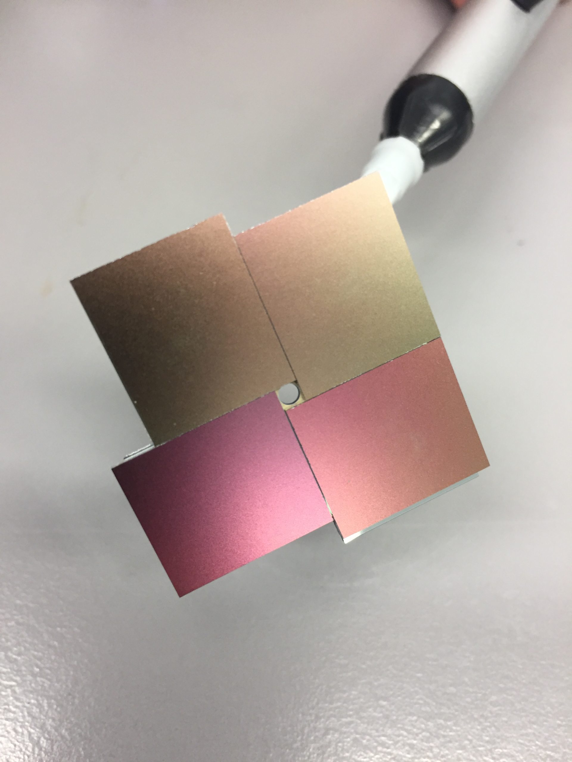
Micromachining of semiconductors
The new technology of laser cutting, drilling and micromachining of semiconductors used in sensors:
– Process without affecting sensor characteristics such as leakage current
– The ability to process the sensor on the entire assembly (ROC+Sensor) without damaging neighbouring pixels
– The thickness of the machined material from 100, 300 to 500 µm
– The possibility of arbitrary sensor shape
– Wafer formatting
– Fabrication of microstructures for controlled change of surface properties (adhesion, increasing of active area)